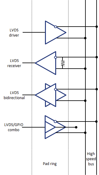
IO cell combining an LVDS receiver, driver or transceiver with a double CMOS GPIO


Description:
A combo cell is an IO cell combining an LVDS receiver, driver or transceiver with a double CMOS GPIO (in, out or bidirectional) powered at 2.5V/1.2V or 1.8V/1.2V, designed on the TSMC 65 LP technology.
Applications:
Multi-purpose reconfigurable IO
Point-to-point, point-to-multipoint or bus-based IC high-speed data communications
Intra-package (e.g. MCM or SIP) inter-die high-speed data communications
Backplane high-speed data communications
High-speed serial communications (HDMI, SATA, PCIeX, etc.)
Communication to LCD/OLED screens
Video sensor digital data interface
Main features:
Standard-compliant to TIA/EIA-644-A-2001
Built-in, low parasitic ESD protection
Easily integrates with TSMC I/O library cells
All-in-ring® topology, so no core silicon area is used by LVDS
The same cells operate with 2.5V/1.2V or 1.8V/1.2V power supplies
Adjustable output common mode voltage (LVDS or SubLVDS mode)
Adjustable driving current for buses with single or double termination
Adjustable output driving current for CMOS GPIOs
Standby/power down mode
Internal bias voltage generation and bias current distribution circuitry
Selectable on-chip termination resistor, with optional user tuning
Digital loopback functions to ease ATE testing
Up to 2 Gbps data rate LVDS
Product brief:
Main characteristics:
2.5V/1.2V IO/Core transistors
Fully compliant with TIA/EIA-644-A-2001
TSMC 65 LP
Deliverables:
GDS II layouts
LEF abstracts
CDL netlists
Liberty timings
Verilog description
A full datasheet
An integration note
Status:
Silicon proven
Radiation proven:
No
Automotive grade:
No


